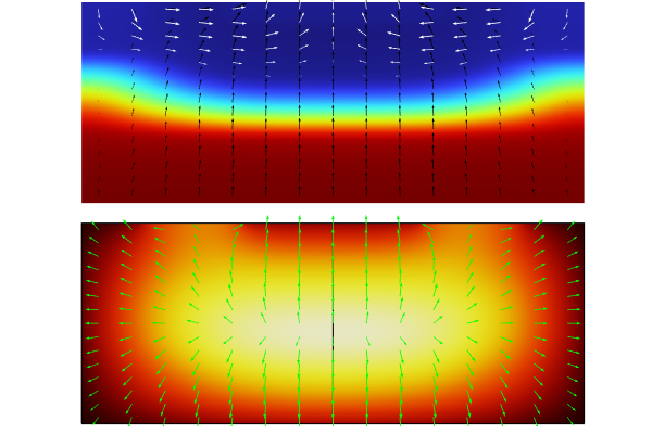
Modeling Semiconductor Contacts
In Part 2 of this course on semiconductor modeling, we expand on the different semiconductor contacts. First, we will show how to simulate a semiconductor diode. The doping of each region is determined by the impurities that are added to the semiconductor during the manufacturing process. Following this, we cover two different methods to simulate insulator-semiconductor contacts, a Thin Insulator Gate boundary condition, and a Charge Conservation domain combined with Insulator Interface boundary condition.
Demo: Heterojunctions
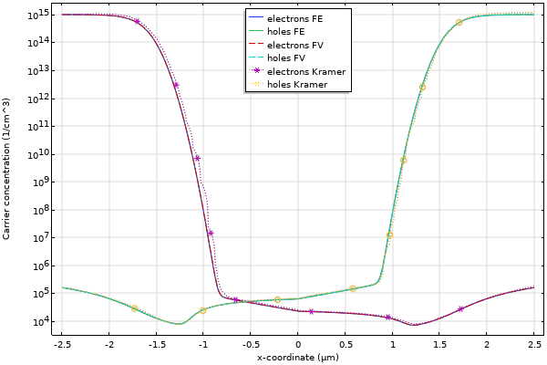
We begin with demonstrating how to set up p-n junction and heterojunction models in the software, highlighting the differences. You will see the complete process for modeling semiconductor-semiconductor contacts and see some alternate methods to achieve the same results. We will observe the behavior of the p-n junction under a reverse, equilibrium, and forward bias. A Shockley–Read–Hall recombination feature is also added to the model to simulate the recombination that is typically observed in indirect band-gap semiconductors, such as silicon.
Discussion and Demo: Semiconductor-insulator Contacts and Transistors
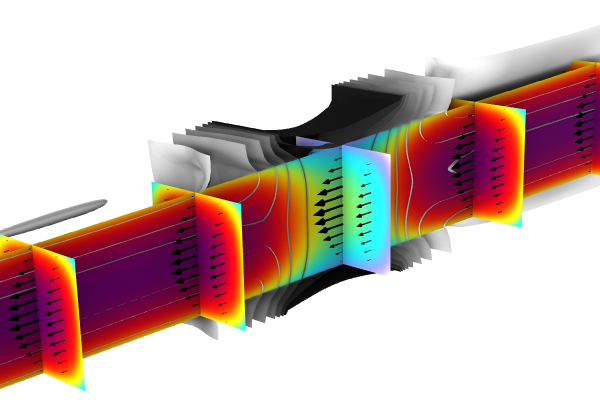
We continue with covering how to model semiconductor-insulator contacts in the software using the metal-silicon-oxide capacitor (MOSCAP) tutorial model. The MOS structure is an essential part for many silicon planar devices. This model uses both a stationary and time dependent study to observe the applied time-varying voltage, the reasons for which are discussed during the demonstration. You will see the model-building process from start to finish and see a few different ways of building the model, such as with a thin insulator gate and charge conservation domain. When using a Thin Insulator Gate boundary condition, the oxide is treated like a thin layer and is not explicitly modeled. When using a Charge Conservation domain, the electric field in the insulator is explicitly modeled and is then coupled as a external electric field onto the surface semiconductor. We also introduce the metal-oxide-semiconductor field-effect transistor (MOSFET) modeling exercise for you to practice on your own.
Modeling Exercise
At the end of the above video (22:49), we introduce a modeling exercise. To gain hands-on experience with the topics discussed here, complete the following exercise with the MOSFET demo model:
- Starting with a blank model, reproduce the MOSFET model. You can build the model completely from scratch or use the parameter list and geometry files below.
- Parameters: mosfet_parameters.txt
- Geometry: mosfet_geometry.mphbin
- Documentation: models.semicond.mosfet.pdf
- Plot the results
- The current at the drain contact (Id) with respect to the voltage of the gate contact (Vg) where the drain voltage (Vd) in 0.01 V.
- The current at the drain contact with respect to the drain voltage at various gate contact voltages
You can manually check your implementation with the solution model files provided here or you can use the comparison tool to identify the differences.
Submit feedback about this page or contact support here.

