FEM and Equivalent-Circuit Modeling of a Thin-Film BAW Resonator
Thin-film bulk acoustic wave resonators, or FBARs, are MEMS components in narrow band filters used in RF applications. Their chief advantage over traditional electronic resonators is their much smaller size. As a result, they have become important building blocks of systems found in mobile devices. In the device design phase, finite element method (FEM) modeling can be used to compute eigenfrequencies, eigenmodes, and frequency responses with the goals to maximize the quality of the main component and reduce the effect of spurious modes. In the subsequent circuit design phase, these FBARs must be represented by equivalent circuits with lumped parameters, because to extend the FEM to model complex circuits would be computationally costly and inefficient. Here, we outline the steps to go from the FEM model to a lumped parameter model in COMSOL Multiphysics®. Building a FEM model of an FBAR and then, from that model, deriving a compact circuit model for system-level simulations is achieved through these primary steps:
- Model a 3D thin-film BAW resonator
- Set up an equivalent-circuit model with lumped parameters
- Determine the values of the lumped parameters using a Parameter Estimation study
FEM Model of the FBAR
To model an example thin-film BAW resonator, based on an anchored five-sided apodized FBAR design for maximizing confinement of vibrational energy, we need the Electrostatics and Solid Mechanics interfaces and the Piezoelectricity coupling. Implementing these features can quickly be accomplished b y selecting the Piezoelectricity, Solid multiphysics interface in the Model Wizard (Figure 1). This single selection automatically adds the required physics interfaces and coupling.
Note: The Application Gallery includes the model file and tutorial documentation for the Thin-Film BAW Resonator with Equivalent Circuit model discussed here. The documentation outlines the steps to build the model, including creating the geometry through completing a parameter estimation study to determine the values of lumped parameters.
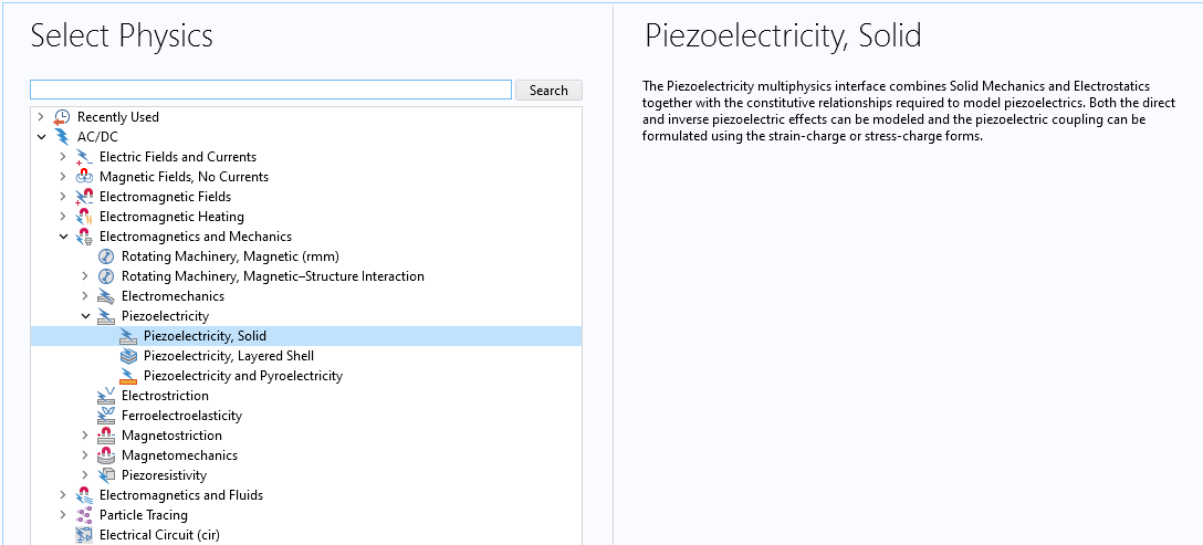 The Select Physics window with the Piezoelectricity, Solid interface highlighted.
Figure 1. Piezoelectricity multiphysics is chosen from the Select Physics window in the Model Wizard.
Due to the symmetry of the device's structure and the mode of interest, only a 36-degree sector needs to be modeled (see Figure 2), which reduces the computational time significantly. This is discussed in detail in our Learning Center entry on using symmetry to reduce model size. This is a good strategy to use in this particular model, where a fine mesh is needed to compute the eigenfrequency and generate a smooth surface plot of the mode shape. The FBAR is designed to have a series resonance at about 3.25 GHz and consists of a 0.2- µm silicon nitride supporting layer, a 0.1- µm molybdenum bottom electrode, a 1- µm aluminum nitride piezoelectric layer, and a 0.2- µm aluminum top electrode. The FEM model is used to compute the frequency response of the device via a Frequency Domain study. In the following steps, this FEM data is used as reference for the experimental data.

Figure 2. 36-degree sector of the five-sided thin-film BAW resonator.
The FBAR modeled here is based on aluminum nitride, which is found under the Piezoelectric branch of the material libraries available with the MEMS Module, as shown in Figure 3. Adding the material to the model enables you to then edit its properties displayed in the Settings window, as shown in Figure 4.

Figure 3. The Piezoelectric material library.

Figure 4. The Settings window displaying the material properties for aluminum nitride.
To obtain the frequency response of the FBAR, we need to run the Frequency Domain study. Its setup is shown in Figure 5. Figure 6 shows the absolute value of the terminal current as a function of frequency from the Frequency Domain study between 2.8 and 3.8 GHz. The series resonance frequency at 3.25 GHz corresponds to the thickness-extension mode.

Figure 5. The settings for the Frequency Domain study for the FEM model.

Figure 6. Frequency response from FEM modeling.
The Modified Butterworth–Van Dyke Equivalent Circuit Model
An electromechanical device such as the FBAR can be represented by the modified Butterworth–Van Dyke (mBVD) circuit with six lumped elements illustrated in Figure 7. The circuit is essentially the aluminum nitride capacitance, Co, in parallel with the series circuit Rm-Lm-Cm (the motional branch) for the piezoelectric effect. The Electrical Circuit interface is used to specify and excite the circuit using the initial values listed in Table 1. These values are estimated using equations in Ref. 1 and are based on the resonance and antiresonance frequencies of the FEM model and the Co value from the device geometry. As in the FEM model, the circuit model is used to compute the frequency response of the device using a Frequency Domain study. With the appropriate initial values, the frequency response from the FEM and circuit model should be close.

Figure 7. Diagram of the mBVD circuit model.
Initial Values Used in the Circuit Simulation
| Name | Initial Value | Description |
|---|---|---|
| Cm | 62 fF | Capacitor, motional |
| Lm | 39 nH | Inductor, motional |
| Rm | 1 ohm | Resistor, motional |
| Co | 1 pF | Capacitor |
| Ro | 500 ohm | Resistor |
| Rs | 1 ohm | Resistor, series |
| Vsrc | 5 V | Voltage source |
Table 1.
To add an equivalent-circuit model, we first add the Electrical Circuit interface, as shown in Figure 8. Next, we add individual circuit components and define their network connection and enter the values of the lumped parameters, as shown in Figure 9.

Figure 8. The Add Physics window, where we select the Electrical Circuit interface to create the equivalent-circuit model of the FBAR.

Figure 9. The Settings window for a circuit component where we specify its circuit connection and the values of its lumped parameter.
A second Frequency Domain study analyzes the frequency response of the circuit as defined by the parameter initial values listed in Table 1. Here, we use the same frequency range as the previous study. Figure 10 shows the plot for the circuit simulation superimposed onto the plot from the FEM simulation.

Figure 10. Plot of current versus frequency from FEM simulation and circuit simulation using the parameter initial values.
Parameter Estimation Study
To derive the precise values of the model parameters, use a Parameter Estimation study. In the Parameter Estimation study, a model expression is computed from the Frequency Domain study of the circuit model defined by the six parameters, which are varied to fit the experimental data (from FEM). To fit the model expression to the experimental data, parameter estimation minimizes an objective function defined as the error between the model expression and experimental data. The setup of the Parameters Estimation study is shown in Figure 11. Another frequency response plot is automatically generated for visualizing the quality of the fit, as shown in Figure 12. The output of the Parameter Estimation study is the set of circuit parameters that best approximates the frequency response from FEM, as summarized in Table 2.

Figure 11. The output of the Parameter Estimation study comparison between experimental data and model expression. The fitted parameters are listed in Table 2.

Figure 12. Plot of the FEM result and equivalent circuit using final parameters from the Parameter Estimation study.
Values of Circuit Parameters Computed from the Parameter Estimation Study
| Name | Initial Value | Description |
|---|---|---|
| Cm | 62.486 fF | Capacitor, motional |
| Lm | 37.177 nH | Inductor, motional |
| Rm | 0.325 ohm | Resistor, motional |
| Co | 1.043 pF | Capacitor |
| Ro | 500 ohm | Resistor |
| Rs | 0.866 ohm | Resistor, series |
| Vsrc | 5 V | Voltage source |
Table 2.
Figure 13 is the surface plot of solid displacement showing the mode shape at 3.25 GHz from a separate FEM eigenfrequency study. This mode corresponds to the peak shown in Figure 12. Note that for high-resonance devices, an eigenfrequency study often returns many solutions that are very close to the resonance frequency at 3.25 GHz. These are called spurious modes and need to be discarded based on visual inspection. As an alternative to visual verification, you can compute the displacement phase uniformity and plot against frequency. For the true resonance, the value will be close to 1, whereas for spurious modes they will be much smaller than 1. A plot of displacement phase uniformity versus frequency is shown in Figure 14.

Figure 13: Surface plot showing the pattern of displacement for the thickness-extension mode.

Figure 14: Plot of displacement phase uniformity versus frequency. Its value is close to 1 only at the resonance frequency of 3.2512 GHz.
Reference
- J. D. Larson et al., “Modified Butterworth-Van Dyke circuit for FBAR resonators and automated measurement system,” Proc. IEEE Ultrason. Symp., pp. 863–868, 2000.
Submit feedback about this page or contact support here.