Studying surface plasmon polariton excitation and field profiles using Wave Optics module in COMSOL®
Surface plasmon polaritons (SPPs) are coherent oscillations of electrons at a metal-dielectric interface coupled to electromagnetic fields [1]. SPPs offer highly confined fields resulting in larger field amplitude and enhanced light-matter interactions. Control and manipulation of light and light-matter interactions at the nanoscale with SPPs has resulted in stronger nonlinearities, improved biosensors and potentially, integrated photonics-on-chip for telecommunication applications [2] [3]. Here, SPP excitation across the telecommunication wavelength (1550 nm) is investigated employing indium tin oxide (ITO) thin film-on-substrate geometry with air/vacuum superstrate as a model. ITO shows tunable plasmonic properties in the IR and is materially compatible with semiconductor manufacturing technologies [4]. Significantly, ITO possesses unique optical properties that allow direct free-space excitation of SPPs. We investigate this important advancement in sub-wavelength light coupling that overcomes the traditional hurdles of SPP excitation using bulky prisms or patterned gratings.
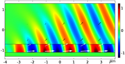
The proposed geometry is probed using plane waves incident from air onto an ITO film on Au. The excited modes are strongly confined within the thin film, with the electromagnetic fields showing evanescent decay on either side of the ITO-metal interface. The mode dispersion, dictated by the permittivity of ITO, is spectrally contiguous to the epsilon-near-zero (ENZ) wavelength of ITO i.e. wavelength at which the real part of permittivity goes to zero [4]. Importantly, the SPPs have mode indices less than 1, validating their excitability from free space (n = 1) with their surface confined propagation verified by calculating the Poynting vector at suitable boundaries. In summary, direct coupling of free-space radiation to SPPs using a thin film of ITO on Au is demonstrated in COMSOL® and detailed analysis of mode dispersion and field profiles are presented to verify the surface mode characteristics.
Modelling details
Electromagnetic field distribution, reflectance/transmittance and eigenmodes are simulated with the ‘Electromagnetic Waves Frequency Domain’ physics interface of the Wave Optics module in COMSOL®, using Wavelength Domain and Boundary Mode Analysis study steps. Simulations are set up following Fresnel equation and Dielectric slab Wave Guide models from Application Libraries. The 2D simulation region is bounded by periodic ports and Floquet boundaries. Evanescent field decay is characterized by line profiles of electric field and propagation is verified by the normalized integrated Poynting vector along the interface. Reflectance minima calculated from S parameters, as a function of wavelength and incident angle using parameter sweeps, trace the SPP dispersion relation. SPP effective index is extracted from Boundary Mode Analysis of the 1D cross-section of the model and used to verify the dispersion relation. A Wavelength Domain study step then visualizes propagation of the calculated modes along the interface. Numerical results and simulation methodology are validated by characterizing SPP excitation in the Kretschmann configuration with plane waves injected through a glass substrate.
References
[1] S. A. Maier, Plasmonics: Fundamentals And Applications (Springer, New York, U. S. A, 2007).
[2] E. Ozbay, Science 311, 189 (2006).
[3] V. Kalathingal, P. Dawson, and J. Mitra, submitted (2019).
[4] G. V. Naik, V. M. Shalaev, and A. Boltasseva, Adv Mater 25, 3264 (2013).

Herunterladen
- COMSOL_Bangalore_2019_BenJohns.pdf - 0.88MB
