Photoresist Spin Coating Simulation
Application ID: 121451
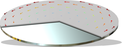
In the semiconductor manufacturing process, photoresist coating is an important process and the thickness of the photoresist layer needs to be precisely controlled. Usually, the photoresist layer is thinned by spin coating. The specific principle is to use centrifugal force to throw excess photoresist away from the wafer surface and generate a specific thickness of photoresist layer by adjusting the material properties and rotating speed, among other things.
This example model simulates the thinning of the photoresist layer through 2D axisymmetric modeling, utilizing swirl flow in the Laminar Flow interface and Free Surface feature. The first transient study calculates the variation of photoresist thickness (initial 10 um) within 120 s at 2 mPas and 8000 rpm. The second transient study uses a parametric sweep to calculate the photoresist thickness at different viscosities and speeds.
The results show that:
- The photoresist layer gradually thins as the wafer rotates, and the thickness is consistent with theoretical results (Emslie, Bonner, and Peck Model).
- The smaller the viscosity, the faster the rotational speed, and the thinner the photoresist layer.
Notes:
- Photoresist is treated as a Newtonian fluid without considering shear thinning or thickening effects and the influence of temperature on viscosity. If there is a non-Newtonian effect, a non-Newtonian constitutive should be used.
- The evaporation of photoresist solvent has not been considered. If necessary, the evaporation flux can be added to the flux on the Free Surface feature.
- The nonslip boundary conditions that are used to treat the contact surface between the photoresist and silicon wafer may require the selection of other wall conditions if there is slip behavior.
Dieses Beispiel veranschaulicht Anwendungen diesen Typs, die mit den folgenden Produkten erstellt wurden:
Allerdings können zusätzliche Produkte erforderlich sein, um es vollständig zu definieren und zu modellieren. Weiterhin kann dieses Beispiel auch mit Komponenten aus den folgenden Produktkombinationen definiert und modelliert werden:
Die Kombination von COMSOL® Produkten, die für die Modellierung Ihrer Anwendung erforderlich ist, hängt von verschiedenen Faktoren ab und kann Randbedingungen, Materialeigenschaften, Physik-Interfaces und Bauteilbibliotheken umfassen. Bestimmte Funktionen können von mehreren Produkten gemeinsam genutzt werden. Um die richtige Produktkombination für Ihre Modellierungsanforderungen zu ermitteln, lesen Sie die Spezifikationstabelle und nutzen Sie eine kostenlose Evaluierungslizenz. Die COMSOL Vertriebs- und Support-Teams stehen Ihnen für alle Fragen zur Verfügung, die Sie diesbezüglich haben.